
|
|||||||
|
|||||||

|
|
|
|||||||
|
|||||||
|
|
| MCD132-08io1资料 | |
|
|
MCD132-08io1 PDF Download |
|
File Size : 116 KB
Manufacturer:IXYS Description: The IDT72T4088/72T4098/72T40108/72T40118 are exceptionally deep, extremely high speed, CMOS First-In-First-Out (FIFO) memories with the ability to read and write data on both rising and falling edges of clock. The device has a flexible x40/x20/x10 Bus-Matching mode and the option to select single or double data rates for input and output ports. These FIFOs offer several key user benefits: • Flexible x40/x20/x10 Bus-Matching on both read and write ports • Ability to read and write on both rising and falling edges of a clock • User selectable Single or Double Data Rate of input and output ports • A user selectable MARK location for retransmit • User selectable I/O structure for HSTL or LVTTL • The first word data latency period, from the time the first word is written to an empty FIFO to the time it can be read, is fixed and short. • High density offerings up to 5Mbit • High speed operation of up to 250MHz Bus-Matching Double Data Rate FIFOs are particularly appropriate for network, video, telecommunications, data communications and other applica- tions that require fast data transfer on both rising and falling edges of the clock. This is a great alternative to increasing data rate without extending the width of the bus or the speed of the device. They are also effective in applications that need to buffer large amounts of data and match buses of unequal sizes. Each FIFO has a data input port (Dn) and a data output port (Qn), both of which can assume either a 40-bit, 20-bit, or a 10-bit width as determined by the state of external control pins Input Width (IW), Output Width (OW), and Bus- Matching (BM) pin during the Master Reset cycle. The input port is controlled by a Write Clock (WCLK) input and a Write Enable (WEN) input. Data present on the Dn data inputs can be written into the FIFO on every rising and falling edge of WCLK when WEN is asserted and Write Single Data Rate (WSDR) pin held HIGH. Data can be selected to write only on the rising edges of WCLK if WSDR is asserted. To guarantee functionality of the device, WEN must be a controlled signal and not tied to ground. This is important because WEN must be HIGH during the time when the Master Reset (MRS) pulse is LOW. In addition, the WSDR pin must be tied HIGH or LOW. It is not a controlled signal and cannot be changed during FIFO operation. Write operations can be selected for either Single or Double Data Rate mode. For Single Data Rate operation, writing into the FIFO requires the Write Single Data Rate (WSDR) pin to be asserted. Data will be written into the FIFO on the rising edge of WCLK when the Write Enable (WEN) is asserted. For Double Data Rate operations, writing into the FIFO requires WSDR to be deasserted. Data will be written into the FIFO on both rising and falling edge of WCLK when WEN is asserted. The output port is controlled by a Read Clock (RCLK) input and a Read Enable (REN) input. Data is read from the FIFO on every rising and falling edge of RCLK when REN is asserted and Read Single Data Rate (RSDR) pin held HIGH. Data can be selected to read only on the rising edges of RCLK if RSDR is asserted. To guarantee functionality of the device, REN must be a controlled signal and not tied to ground. This is important because REN must be HIGH during the time when the Master Reset (MRS) pulse is LOW. In addition, the RSDR pin must be tied HIGH or LOW. It is not a controlled signal and cannot be changed during FIFO operation. Read operations can be selected for either Single or Double Data Rate mode. Similar to the write operations, reading from the FIFO in single data rate requires the Read Single Data Rate (RSDR) pin to be asserted. Data will be read from the FIFO on the rising edge of RCLK when the Read Enable (REN) is asserted. For Double Data Rate operations, reading into the FIFO requires RSDR to be |
|
| 相关型号 | |
| ◆ R3968FD28N | |
| ◆ R3968FD28R | |
| ◆ R3968FD28T | |
| ◆ R2619ZC25J | |
| ◆ R3370ZC12D | |
| ◆ R600CH25 | |
| ◆ N0734YS160 | |
| ◆ N540SH18 | |
| ◆ N540CH18 | |
| ◆ R355CH12 | |
| 1PCS | 100PCS | 1K | 10K | ||
| 价 格 | |||||
|
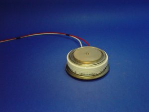
型 号:MCD132-08io1 厂 家:IXYS 封 装:模块 批 号:new 数 量:1500 说 明: 原装正品、长期现货、三包承若 所报价格均含税含运费价格!如果不明白欢迎来电咨询,谢谢! 特征 芯片与底板电气绝缘
交直流电机控制 标准二极管模块 应用: |
|||||
|
运 费:10.00元(快递) 所在地:昆山市 新旧程度:全新 |
|||||
| 联系人:林志胜 |
| 电 话:4006333495,0512-50111678 |
| 手 机:18602223500,18962647678 |
| QQ:5178133,4006333495 |
| MSN: |
| 传 真:0512-82092268(自动),50111789(手动) |
| EMail:qiwodz@vip.qq.com |
| 公司地址: 江苏省昆山市开发区前进东路233号 |
|
江浙沪地区:首重1KG 5.00 元 续重1KG 1.00元 其他地区:首重 1KG 10.00元 续重1KG 5.00元 如需顺丰快递请在订购前说明,谢谢! |