
|
|||||||
|
|||||||

|
|
|
|||||||
|
|||||||
|
|
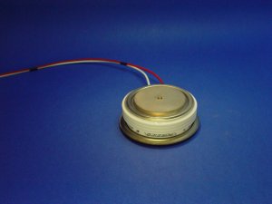
| MDD95-20N1B资料 | |
|
|
MDD95-20N1B PDF Download |
|
File Size : 116 KB
Manufacturer:WESTCODE Description:SIGNAL DESCRIPTIONS See Figure 1, Logic Diagram, and Table 1, Signal Names, for a brief overview of the signals connect- ed to this device. Address Inputs (A0-A17). The Address Inputs select the cells in the memory array to access dur- ing Bus Read operations. During Bus Write opera- tions they control the commands sent to the Command Interface of the internal state machine. Data Inputs/Outputs (DQ0-DQ7). The Data In- puts/Outputs output the data stored at the selected address during a Bus Read operation. During Bus Write operations they represent the commands sent to the Command Interface of the internal state machine. Data Inputs/Outputs (DQ8-DQ14). The Data In- puts/Outputs output the data stored at the selected address during a Bus Read operation when BYTE is High, VIH. When BYTE is Low, VIL, these pins are not used and are high impedance. During Bus Write operations the Command Register does not use these bits. When reading the Status Register these bits should be ignored. Data Input/Output or Address Input (DQ15A-1). When BYTE is High, VIH, this pin behaves as a Data Input/Output pin (as DQ8-DQ14). When BYTE is Low, VIL, this pin behaves as an address pin; DQ15AC1 Low will select the LSB of the Word on the other addresses, DQ15AC1 High will select the MSB. Throughout the text consider references to the Data Input/Output to include this pin when BYTE is High and references to the Address In- puts to include this pin when BYTE is Low except when stated explicitly otherwise. Chip Enable (E). The Chip Enable, E, activates the memory, allowing Bus Read and Bus Write op- erations to be performed. When Chip Enable is High, VIH, all other pins are ignored. Output Enable (G). The Output Enable, G, con- trols the Bus Read operation of the memory. Write Enable (W). The Write Enable, W, controls the Bus Write operation of the memorys Com- mand Interface. Reset/Block Temporary Unprotect (RP). The Re- set/Block Temporary Unprotect pin can be used to apply a Hardware Reset to the memory or to tem- porarily unprotect all Blocks that have been pro- tected. A Hardware Reset is achieved by holding Reset/ Block Temporary Unprotect Low, VIL, for at least tPLPX. After Reset/Block Temporary Unprotect goes High, V IH, the memory will be ready for Bus Read and Bus Write operations after tPHEL or |
|
| 相关型号 | |
| ◆ R3968FD28N | |
| ◆ R3968FD28R | |
| ◆ R3968FD28T | |
| ◆ R2619ZC25J | |
| ◆ R3370ZC12D | |
| ◆ R600CH25 | |
| ◆ N0734YS160 | |
| ◆ N540SH18 | |
| ◆ N540CH18 | |
| ◆ R355CH12 | |
| 1PCS | 100PCS | 1K | 10K | ||
| 价 格 | |||||
|
型 号:MDD95-20N1B 厂 家:WESTCODE 封 装:平装 批 号:new 数 量:1200 说 明: 原装正品、长期现货、三包承若 所报价格均含税含运费价格!如果不明白欢迎来电咨询,谢谢! 特征 芯片与底板电气绝缘
交直流电机控制 标准二极管模块 应用: |
|||||
|
运 费:10.00元(快递) 所在地:昆山市 新旧程度:全新 |
|||||
| 联系人:林志胜 |
| 电 话:4006333495,0512-50111678 |
| 手 机:18602223500,18962647678 |
| QQ:5178133,4006333495 |
| MSN: |
| 传 真:0512-82092268(自动),50111789(手动) |
| EMail:qiwodz@vip.qq.com |
| 公司地址: 江苏省昆山市开发区前进东路233号 |
|
江浙沪地区:首重1KG 5.00 元 续重1KG 1.00元 其他地区:首重 1KG 10.00元 续重1KG 5.00元 如需顺丰快递请在订购前说明,谢谢! |


 技术支持:维库电子市场网